DŮVĚŘIVÝ
A computer constructed by blah, in Rychládrát, inspired by Jack Eisenmann, named after the Czech word for computer. My second computer.
Důvěřivý is a simple 8-bit computer. It was designed to be easier to programme than my previous one (Dick), and also more realistic. As such, it uses byte-addressable RAM and follows a more conventional architecture.
Some images of circuits are links; they lead to .rle files containing the circuits they depict. These are plaintext files that can be copied and then pasted into the "save code" box in Reasoning Realm.
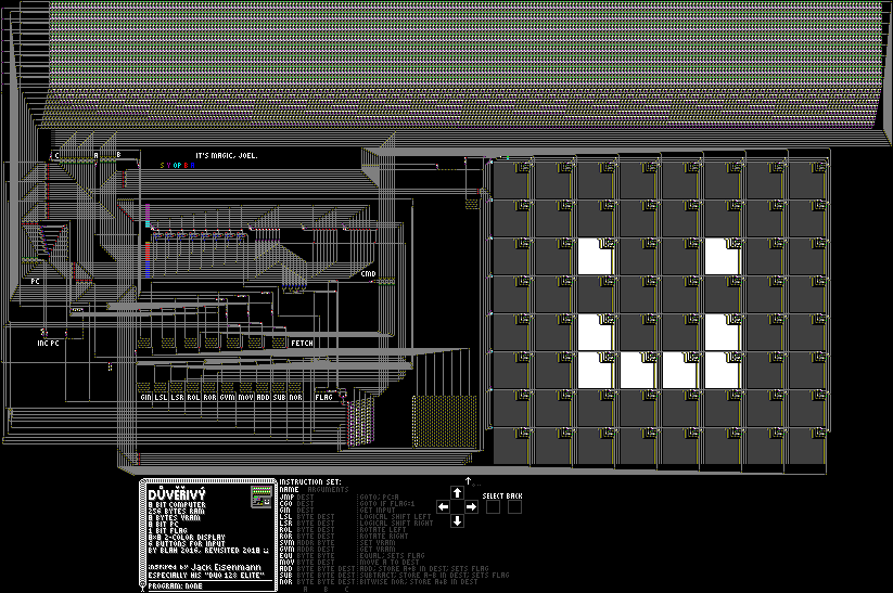
Table of contents
Rychládrát
Důvěřivý was created in Rychládrát, a system in which circuits can be constructed, similar to Logic Land, but with instant wire. As of writing this, it can be simulated only by Reasoning Realm and a Lua script for Golly.
Rules
The simulation consists of a square grid of arbitrary dimensions, in which each square (cell) is in one of the following states:

- Empty Space (#000000)
- Inactive Wire (#404040)
- Active Wire (#FFFFFF)
- Active Gate Output (#252545)
- Inactive NOR Gate (#960096)
- Inactive OR Gate (#969600)
- Inactive AND Gate (#FA0000)
- Inactive NAND Gate (#00FAFA)
- Inactive XOR Gate (#0000FA)
- Inactive Gate Output (#202040)
- Active NOR Gate (#9B059B)
- Active OR Gate (#9B9B05)
- Active AND Gate (#FF0505)
- Active NAND Gate (#05FFFF)
- Active XOR Gate (#0505FF)
- Inactive Switch (#007F00)
- Active Switch (#00FF00)
- Insulated Wire (#7F7F7F)
The simulation takes place in steps, called ticks or generations, in which the state of a cell may change depending on its own state and the state of other cells.

The gate inputs themselves will become either active or inactive depending on the amount of active or inactive wire cells around (see still picture for details). Gate outputs will become active if there are any active gate inputs around, otherwise they will become inactive; when a gate changes state, it emits rays in all 4 directions, see animation. Note that this does not happen when the gate remains in the same state; this is relevant to memory circuits.
In the animation at t=0, you see an active gate output (state 3) surrounded by active wire "state 2". There are no active gate inputs nearby, so the gate output becomes inactive. In doing so it sets all the wires in orthogonal rays around it to be inactive too; this is how signals propagate through wires. In order to turn a signal, another gate is required. The rays emitted by gate outputs stop when they reach any cell which is neither state 1, 2, 16, nor 17. If the gate is inactive becoming active, it will set all state 1 cells in the path of the rays to state 2, and vice versa when going inactive.
Switches (states 15 and 16) are used to selectively allow signals to pass though. A switch will be inactive if there is an inactive gate output nearby, otherwise it will be active. Insulated wire exists to allow for wires which require less effort to compute, since most of the wire is simply iterated through in a for loop without having to set any cells. It can also be used to allow a signal to pass next to a gate input without affecting it.
If you are confused about any of the details and/or want to gain a deeper understanding, I encourage you to play around with Rychládrát in Reasoning Realm.
Architecture
Důvěřivý is an 8-bit computer. The state of the machine at any given time consists of 256 bytes of RAM, 8 bytes of VRAM, an 8 bit PC, a 1 bit flag used for conditional jumping, and it also has 6 bits of input. There are practically no 'registers' in the conventional sense, and so the memory hierarchy for the programmer starts with RAM. The CPU has 14 opcodes. They are as follows:
| name | opcode | operands | writes to RAM? |
function |
|---|---|---|---|---|
| JMP | 00000 | 1: A | No | Sets PC to A |
| CGO | 00001 | 1: A | No | Sets PC to A if the flag is set |
| GIN | 00010 | 1: A | Yes | Write a byte to memory address A containing the states of the 6 input buttons, where the byte is two 0s followed by a bit for each input; 1 if pressed down, otherwise 0. They are ordered as such, from most to least significant bit: BACK, SELECT, RIGHT, UP, LEFT, DOWN. |
| LSL | 10000 | 2: AB | Yes | Perform logical shift left on A, and write to memory address B |
| LSR | 10001 | 2: AB | Yes | Perform logical shift right on A, and write to memory address B |
| ROL | 10010 | 2: AB | Yes | Perform rotate left on A, and write to memory address B |
| ROR | 10011 | 2: AB | Yes | Perform rotate right on A, and write to memory address B |
| SVM | 10100 | 2: AB | No | Set VRAM. The least significant 3 bits of A are used as an address for a row of the display to set, and its contents are set to B. |
| GVM | 10101 | 2: AB | Yes | Get VRAM. The least significant 3 bits of A are used as an address for a row of the display to read, and its contents are read to memory address B. |
| EQU | 10110 | 2: AB | No | Checks if A==B, and sets flag accordingly. |
| MOV | 10111 | 2: AB | Yes | Writes A into memory address B. |
| ADD | 11000 | 3: ABC | Yes | Calculate the sum of A+B, and write result to memory address C. The flag is set to whether or not it overflowed. |
| SUB | 11001 | 3: ABC | Yes | Calculate A-B, and write result to memory address C. The flag is set to whether or not it overflowed (A≥B). |
| NOR | 11010 | 3: ABC | Yes | Calculate bitwise NOR of A and B, and write result to memory address C. |
Arguments can be substituted for contents of locations in memory (represented with square brackets). For example, [0] would return the contents of memory address 0.
The command byte consists of the 5 opcode bits, and then 3 bits specifying whether or not each argument should be substituted with an address in RAM. For example, SVM [0] 12 would be assembled to 10100100 00000000 00001100.
Programmes
DASM
DASM is a simple assembly language I created. It consists, formally, of the following rules:
- Comments are marked with a semicolon.
- Each line contains either data, a label, or nothing.
- Data can either be a number or an assembly instruction.
- Numbers are interpreted as base 16 by default, but if they are 3 digits they are base 10, and if they 8 digits they are base 2. They are always bytes.
- Assembly instructions are formatted as such: (INSTRUCTION) (OPA) (OPB) (OPC), where (INSTRUCTION) is one of the three-character operation names listed above. OPB and OPC are only required for opcodes that have them.
- An operand for the opcode can be either a label (interpreted as the label's address in RAM) or a number formatted as described above. In either case, it can have square brackets placed around it to perform the function described in the 'Architecture' section.
- Labels can be formatted as :(LABEL), where (LABEL) is an arbitrary name. It can then be used as a name for that location in memory (technically it is equivalent to a number, which is the address in memory that the label refers to).
- (LABEL): (DATA) is syntactic sugar for
:(LABEL)
(DATA), which is useful for declaring variables. Note that there must be exactly one space between the colon and the (DATA), no more, no less. - The label called START is used as the starting point of the programme, otherwise the starting point of the programme is the first byte in memory; if your programme begins with instructions, this may be intended behaviour for you anyway.
- (LABEL): (DATA) is syntactic sugar for
Examples
Here are some small examples demonstrating certain properties. For larger programmes see here.
I have written an emulator for Důvěřivý, available here, which can be used to run these examples. The assembled programmes can also be written into the computer itself by using this script in Reasoning Realm with the computer loaded.
Hello World
SVM 0 00000000
SVM 1 01001010
SVM 2 01001010
SVM 3 01111010
SVM 4 01001010
SVM 5 01001010
SVM 6 01001010
SVM 7 00000000
:ENDLOOP
  JMP ENDLOOP
This programme writes the word HI to the display, visually. It should be pretty self-explanatory.
Counter
NUM: 0
:START
  ADD 1 [NUM] NUM ; We add 1 to the variable
  SVM [NUM] [NUM] ; Then write it to the display
  JMP START
This programme declares a variable, NUM, and then increments it while displaying it. This is an important demonstration of how SVM works; if you run it, you will notice that the location it is writing the number to corresponds to the number's value. The least significant 3 bits remain constant after the first time it gets to the bottom of the display, and then the columns to the left start counting in binary themselves.
Screen shifter
LOC: 0
SCREENBYTE: 0
:START
  GVM [LOC] SCREENBYTE        ; Get the row
  ROR [SCREENBYTE] SCREENBYTE ; Rotate it to the right
  SVM [LOC] [SCREENBYTE]      ; And put it back
  ADD [LOC] 1 LOC             ; Increment LOC to move to next row
  JMP START
Going in a loop while incrementing a variable, and shifting rows of VRAM. Note that incrementing a variable requires a 4-byte ADD instruction.
Quine
LOC: 0
:START
  MOV [LOC] 6
  SVM [LOC] [0]
  ADD [LOC] 1 LOC
  JMP START
This is a quine that outputs the full contents of memory and then repeats, using self-modifying code to use the address of LOC as a pointer to a pointer, which would make LOC itself a pointer. Technically, this quine is cheating, since it reads itself from memory rather than producing itself anew.
It modifies the second operand of SVM, which is a location in memory of a byte to display on the screen, by writing [LOC] to it, which then gives us the effect of SVM [LOC] [[LOC]], which would otherwise be impossible. This is done by the MOV [LOC] 6 instruction, which requires counting the amount of bytes from the beginning of memory to that operand itself.
Components
RAM/VRAM
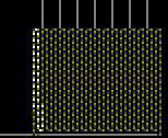
The basic design for the RAM consists of the following, where (for byte-addressable memory) READ, WRITE and DATA each consist of 8 wires, corresponding to each bit of a byte:

The DMUX (demultiplexer) selects a byte of RAM, specified by ADDR (address). If all 8 READ wires are activated, only the wires whose corresponding bit in the selected byte is a 1 will allow a signal to fully reach the other side (OUT), and as such OUT contains the stored data. We will get into writing later, but first let's examine ROM.
Reading

Shown to the left is 2 bits stored in ROM units. The lower unit contains 0, and the upper unit contains 1. The data itself is stored in the lower right cells; state 2 if the bit is a 1, state 1 if it is a 0. The READ signal goes through the top row of the unit design; if a bit is 0, the switch will be inactive, thus preventing a signal from passing, otherwise the signal will be able to pass.
The vertical wire section on the left of the design allows for only one byte of memory to be selected; if that wire contains state 2, the switches will always be on, and as such you only read the column you intend to. Here's a demonstration:
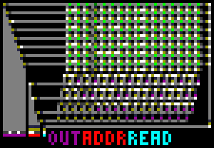
In this case, the READ signal is being sent from the right. The demultiplexer is a simple component that checks for various combinations of the address bits; here we see it selecting column 0011 (3). The read signal is deactivated before the address is changed, in order to ensure that bits in the output wires set to 1 don't remain 1 even if they should be 0.
The 8 READ wires are either all off, or all on, at any given time. The same is true of WRITE; however, DATA contains the byte to be written.
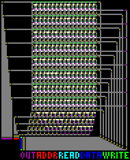
Writing
Here is a single RAM unit, with all 4 input wires extended by two cells in arbitrary directions.

At the top, we see the normal ROM design, with its read signal; below it, we see a mechanism for modifying the state of the cell that dictates the state of the ROM unit. The wire that feeds into the NOR gate is the WRITE wire, and the one below is the DATA wire. The WRITE stream is usually active, so its inputs are inverted in practice; as such, we will say that WRITE is active only when the cells in its stream are inactive wire. To write data, these steps are followed:
- Activate WRITE. This will turn on the lower switch of the RAM unit if it is in the selected byte.
- Activate DATA. The cell that actually stores the bit is now active wire.
- If you wish to write a 0 to any given bit, deactivate DATA.
- Deactivate WRITE.
- Deactivate all DATA wires.
That process could be modified slightly in some ways, but this is how it is used in Důvěřivý. Here is an example of RAM:
VRAM/Display
The VRAM is simply a version of the RAM which is modified to have the stored bit lead to a series of OR gates which carry it out over a large area. As such, the VRAM does not lead to a display, it simply is a display.
The larger memory cell size means that the DMUX was designed completely differently, since it does not have the same space (or address size) requirements; it is similar to the DMUX used in the ALU for the opcode, except it uses NAND gates instead of AND gates. I could've used NOR gates but I wanted an excuse to use NAND gates; the 8 NAND gates used in the VRAM DMUX are the only NAND gates in the entire computer that serve a functional and not visual purpose.
Registers
The computer uses the following design for a register:

First the WRITE wire is activated; this will turn on the switches, and then it flashes all 8 bits to reset their values to 0s, using a monostable circuit. Then the DATA stream can be used simply to write to the register itself.
The computer has 4 'registers' that each store 8 bits, referred to as A, B, C, CMD, and PC. Aside from the PC, none of the registers are intended to store any information between CPU cycles; they are simply intended to store the command byte and its operands. The command byte is stored in CMD, and the operands are stored in A, B, and C.
Uses of each register
The registers are attached to various components; A, B, and C can be fed to the left into the address bus leading into the RAM DMUX, so that the operands can be substituted with a location in memory. The rest of the uses of the three argument registers A, B, and C correlate with the opcodes described in the 'Architecture' section: A leads into the PC, for JMP and CGO, A and B both lead into the ALU for LSL, LSR, ROL, ROR, EQU, ADD, SUB, and NOR; A leads directly into the RAM DATA bus for MOV, A leads ino the VRAM DMUX for SVM and GVM, B leads into the VRAM DATA bus for SVM, and the connections to the RAM DMUX address bus are used for output in GIN, LSL, LSR, ROL, ROR, GVM, MOV, ADD, SUB, and NOR.
CMD leads into the control unit, and the details of its use will be described further later on.
Programme Counter
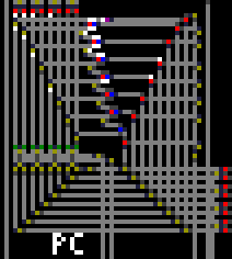
The PC (Programme Counter) leads into the RAM DMUX and has a write bus leading into it which can be filled from two sources: A (used by JMP and CGO), or the output of an incrementer circuit, seen in full in the image above. The incrementer circuit is used every time one of the 2 to 4 instruction bytes is fetched from memory. Below the PC is the circuitry that increments it:

If you set the rightmost non-state-0 cell in the above picture to active wire, the PC will be incremented. This consists of the normal register-WRITE circuitry on the left, and from the right a signal is sent up that allows the incrementer's output to lead into the PC.
ALU
The ALU consists of the inputs (A and B) being run through multiple different operations simultaneously, and, according to the opcode, only one of the operations will have its result fed into the overall output of the ALU. There is also a status input (S), which can be used for a few purposes. Here it is with A=5 and B=31:

The main input and output wires are marked on the left. Blue is A, red is B, the opcode is light blue, the output is purple, and the other wire is the status input. There are 4 meaningful opcodes (meaningless opcodes will result in all 0s for output):
| opcode | output |
|---|---|
| 000 | A+B if S=0, else A+B+1 |
| 001 | A bitwise NOR B |
| 011 | Logical shift right of A if S=0, else rotate right |
| 100 | Logical shift left of A if S=0, else rotate left |
There are 3 bits for the opcode, even though only 2 are necessary. I believe I originally intended to have a bitwise XOR (which would've been a good idea), but decided against it, and forgot to change the amount of opcode bits accordingly.
Speaking of mistakes, the ripple-carry adder-subtractor component uses the status input as its carry-in input, which is used exclusively by SUB. However, in order for an adder-subtractor circuit to go from addition to subtraction, one input must be inverted and the carry-in input must be enabled. As such, the SUB opcode's wiring sends its own signal up to the adder-subtractor in order to invert one input; it would make more sense if the status input did this too, but I do not care enough to make that change, since the problem does not affect the functioning of the computer.
The other components, from left to right, are a simple bitwise NOR, an equality test at the bottom which takes the collective OR of the XORs of all the corresponding bits in the two bytes (used for EQU), and two shifter/rotator components.
There are two wires from the ALU that can lead into the flag, one from the carry-out of the adder-subtractor, and one from the equality test. They are used by ADD and SUB, and EQU, respectively.
Control Unit (CU)
The design process for the computer consisted of creating simple components that can have their inputs manipulated in order to make them perform some kind of simple function, and then creating circuitry that can allow you to activate just one wire, and the inputs to the component will be toggled in just the right way to perform its function.
This encapsulation eventually lead up into larger and larger components with collectively fewer and fewer inputs, until at the end there were 8 wires which could be activated in sequence to perform an entire CPU cycle, and then a simple clock was placed to automate even that. As a whole, the CU was the last part of the computer which was made.
It executes the following interpretation of the command byte's bits, listed here from most to least significant:
![A diagram of the 8 bits of the command byte, where the first 2 bits are labeled B and C, the last three bits are labeled [A], [B], and [C], and the first five bits all comprise the opcode.](/assets/důvěřivý/commandbytediagram.png "doot")
The first 2 bits indicate whether there are B and C operands; operand A is assumed, as all instructions have 1, 2, or 3 operands. It would be possible for there to be an opcode with a C operand but no B operand, although this was not done.
The last three bits are whether or not to substitute an operand for a RAM address. They are represented by square brackets in assembly.
If you happen to be Jack Eisenmann - and you probably aren't - this may seem reminiscent of the DUO Adept's machine code. This is not a coincidence; the input and output may have been inspired by the DUO 128 Elite, but the computer itself is much closer to the DUO Adept.
Given the way this is implemented, invalid opcodes have clear deterministic behaviour: They will take an amount of operands proportional to the amount of the first two bits that are 1, but perform no operation. This knowledge is useful if you want to make a comprehensively accurate emulator or use NOP opcodes.
Clock
The clock executes a single CPU cycle by activing 8 wires in sequence, which perform the following functions:
- Read CMD byte.
- Read argument A.
- Read argument B if needed.
- Read argument C if needed.
- Substitute A with location in memory if needed.
- Substitute B with location in memory if needed.
- Substitute C with location in memory if needed.
- Execute command.
Steps 1, 2, 3, and 4, all increment the PC, with the exception that 3 and 4 do not increment the PC if nothing is read from memory.
Much like my first computer, the clock was the last component to be added, and because I simply wanted to get the computer to finally work it is incredibly simplistic and unoptimised. Timing to me was always the most frustrating part of computer design.
FETCH Coils
The first 7 of the clock's outputs lead into these coils, which fetch the command to be executed and its operands. The coils themselves are to add a delay whilst the RAM DMUX operates.
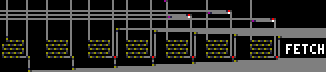
These components are difficult to capture in a single picture, since - like most of the CU - their wires are not all contained in a single area, so I will simply attempt to explain what they do over all. If you wish to examine exactly where these events occur, I recommend observing the computer in action.
Initial FETCH Coils
The leftmost 4 coils read bytes into registers by going through the following process:
- Activate WRITE input of register, and move PC into address bus.
- Wait for the RAM DMUX to operate.
- Activate RAM READ input.
- Wait for input from clock to return to 0.
- Deactivate WRITE, take PC out of address bus, and increment PC.
The coils to fetch B and C are conditional; there are AND gates using the 2 most significant bits of CMD that either allow or do not allow B and/or C to be fetched.
Argument Substitution Coils
The rightmost 3 coils substitute arguments for locations in memory and are also conditional. They work as such:
- Put register into address bus.
- Wait for the RAM DMUX to operate.
- Take register out of address bus. This will take a while to propagate into the DMUX itself, so the other two steps can still occur.
- Activate RAM READ signal for 1 gate delay (2 ticks).
- Activate WRITE to the register for a short period of time, such that the OUT signal from RAM reaches the register just as it is about to close.
The last 3 steps occur almost simultaneously, and have very sensitive timing.
Instruction Decoder

The 5 opcode bits of CMD lead into the instruction decoder, which uses the same design for a demultiplexer as RAM except it's not enumerating all possible inputs, only the ones that are valid opcodes, and the outputs are inverted. All 14 outputs lead directly into AND gates where the other input is a pulse from the clock, so when the clock sends a pulse over to the instruction decoder, one (or none, if the opcode is invalid) of the 14 output wires is activated.
The output wires then have their own paths that lead throughout the computer and do whatever they need to do to execute the desired instruction. They are listed here from top to bottom.
| command | function |
|---|---|
| JMP | Activate part of the INC PC wire, namely the part that allows PC to be written to, its WRITE input, and send the contents of A into the PC, to be written. |
| CGO | Conditionally activate JMP if the flag is positive. |
| GIN | Put A into address bus, wait for RAM DMUX to operate, then write input to RAM. |
| LSL, LSR, ROL, ROR |
Select corresponding opcode and status input for ALU, put B into address bus, wait for RAM DMUX to operate, write output of ALU to RAM. |
| SVM | Put 3 bits of A into VRAM DMUX, activate VRAM WRITE input, quickly send all 1s through VRAM DATA input, send B into VRAM DATA input, wait for input from clock to end, deactivate VRAM WRITE input, take B out of VRAM WRITE input, take A out of VRAM DMUX. |
| GVM | Put B into address bus, put 3 bits of A into VRAM DMUX, wait for RAM DMUX to operate, activate VRAM READ input and write it to RAM. |
| EQU | Write result of ALU equality test to flag. |
| MOV | Put B in address bus, wait for RAM DMUX to operate, write A to RAM. |
| ADD | Put C in address bus, set flag to carry-out of adder, wait for RAM DMUX to operate, write output of ALU to RAM. |
| SUB | Before command is even executed, turn adder into subtractor by setting status input to 1 and inverting input from B into adder. Once command is executed, put C into address bus and write borrow-out of subtractor (A≥B) to flag, wait for RAM DMUX to operate, write output of ALU to RAM. |
| NOR | Select corresponding opcode and status input for ALU, put C into address bus, wait for RAM DMUX to operate, write output of ALU to RAM. |
Flag

The flag is a simple RS-NOR latch with inputs from the adder circuit and from the equality test (both ALU components). These two inputs can be seen around the top-right of the image, both leading into the same OR gate. The flag also has inputs from the opcodes that use it, which feed through a delay (to wait for the intended new value to arrive) and then modify the RS NOR latch itself, located in the lower right.
I believe the circuitry surrounding the RS NOR latch is technically a gated D latch.
Mistakes
The vast majority of the work on the computer that I did was in 2016. I do not care enough to fix all of the problems at this point; I mostly revisited it in 2018 to work on documentation, so all I will do is explain my mistakes rather than fix them.
One exception is that the SUB opcode previously had an issue where it did not actually set the flag, and this required some very confusing wiring to fix. It would've just been a simple matter of joining the SUB opcode wiring up with some of the ADD wiring, however time must be given for the adder-to-subtractor conversion to ripple down the adder; also see ALU mistake #2.
- The architecture leaves some functionality to be desired:
- It would be very simple and somewhat useful to have an "NCG" (inverted CGO) opcode to simplify some branching, but this was never implemented.
- There is no XOR (see ALU section, #3). As such it takes 5 NOR operations to compute an XOR. As a general word of advice to anybody who intends to create a computer, having only one bitwise logical operation is not a good idea. It's worth the extra effort to add others.
- The architecture is simplistic and inefficient and the memory hierarchy, for the most part, starts and ends at RAM. If I made a similar computer using what I know now, I'd have made use of registers.
- It would be perfectly possible to add more two-operand commands by setting the first two opcode bits to 01, but this was not done. Maybe I would've added more two-operand opcodes if I was aware of this, but I don't remember.
- The computer is incapable of solving the "pointer-to-a-pointer" problem without self-modifying code.
- The ALU has several design flaws (see ALU):
- The ALU has 3 opcode bits, even though it only needs 2.
- The adder-subtractor does not use the status input to fully turn into a subtractor. This is likely the result of a planned add-with-carry opcode that was never implemented.
- There is no XOR. I believe I originally planned to have a bitwise XOR which would also double as the mechanism for EQU, but I then moved the XOR component to the bottom of the ALU and used it solely for EQU.
- The clock is entirely unoptimised; it's simply a coil optionally activating certain parts of the computer, which it waits for even if they are not activated. The simplicity has the benefit of each clock cycle taking the exact same amount of time, which simplifies emulators, but it also reduces the speed of simulation.
- There is a redundant Insulated Wire cell at x=763, y=145.