DICK
A computer constructed in Logic Land, inspired by Jack Eisenmann and the Wireworld computer, named after Richard Stallman (sure). Dan helped but not much.
The page on the Life MRM ends with a comment that I will paraphrase. If even one person reads through this and is inspired to create a computer themselves, it will have been worth writing. It's easier to do than I thought.
HOW TO USE: An emulator is available. If you want to see programmes running on the actual machine, copy this save code into Reasoning Realm, then use this script to write a programme to RAM. If the programme is too large to fit in 32 rows of RAM, use this bigger save code instead.
Table of contents
Logic Land
Logic Land is a cellular automaton (CA) created by Jack Eisenmann. It is complicated but intuitive, so I recommend looking at the example circuits in the linked page to understand how it works, but for reference here is a detailed explanation of the transitions. Feel free to skip this.
Cell states:
- Empty Space (#96E6E6)
- Inactive Wire (#E18032)
- Active Wire (#FFFF00)
- Inhibited Wire (#6E4019)
- Cross Over (#808080)
- Inactive NOR Gate (#960096)
- Inactive OR Gate (#FFFFFF)
- Inactive XOR Gate (#0000FF)
- Inactive AND Gate (#FF0000)
- Inactive T Flip Flop (#008000)
- Inactive Gate Output (#000000)
- Active NOR Gate (#960096)
- Active OR Gate (#FFFFFF)
- Active XOR Gate (#0000FF)
- Active AND Gate (#FF0000)
- Active T Flip Flop (#008000)
- Active Gate Output (#000000)
The neighbours of a cell are the 4 cells with touching sides. This is known as the Von Neumann neighbourhood.

Empty space is inert, it can never do anything.
The first three states allow signals to travel through wire. Inactive wire turns active if it has active wire cells nearby. In this animation we see a wire getting activated. At the end you see that the signals propagate in accordance with discrete manhattan distances, and can only travel through polyominoes.

We need a way to turn active wire inactive, so we add Inhibited Wire. It will convert Active Wire to more Inhibited Wire, then become Inactive Wire.
The animation you see here also demonstrates cross overs. Worth noting about crossovers is that signals travel from one end to the other in one generation, which means if every other cell of a wire is a crossover, signals propagate twice as fast.

That leaves the gate components, which are based on the fact that Inactive Gate Outputs are treated the same as inhibited wire, and active gate outputs are treated the same as active wire. The effect is that any wire attached to a gate output will be bound to the value of that gate output.
The computation happens with the gate inputs. They will be active if there are any active wires nearby, otherwise they become inactive. Whether a gate output becomes active or inactive will depend on the state and type of gate inputs near it. I'm not very good at explaining this, so hopefully the animation I have here and/or your own experimentation in the CA will help you understand.
Additionally, T-Flip-Flops work differently from all the other gate inputs; they will invert their value if there is 1 or more inhibited wire near it.
Architecture
A transport triggered architecture (TTA) is a type of one instruction set computer (OISC). More specifically, it is a case where the only instruction is MOV, which will copy the value at one location into another location. But that's not even turing complete! Unless we have memory-mapped instructions. I'll get back to those.
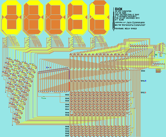
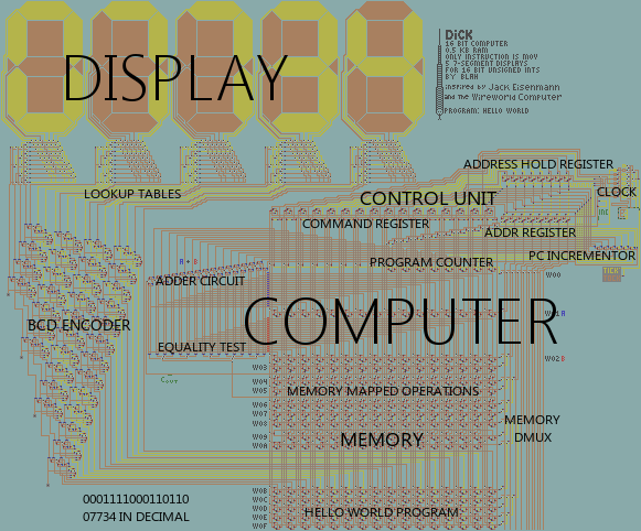
Instructions and data are read from word-addressable RAM, which consists of 256 words (although not all store a full word) of memory addressed by an 8-bit multiplexer. I refer to these words as WXX, where XX is the address in hexadecimal.
Instructions are formatted such that the contents at a memory address specified by the least significant byte of the instruction word is copied to the memory address specified by the most significant byte.
And to get back to memory-mapped instructions, they are addresses in memory that behave differently from the others, in such a way that you can perform computation with them. Here is a table. (nothing is original)
| nickname | W?? | abnormal behaviour |
|---|---|---|
| PC/ABSUM | W00 | Reading returns OPA + OPB, and writing sets the programme counter (PC). Note that the PC is incremented before an instruction is fetched, so to jump to a location X you have to set the PC to X - 1. |
| OPA | W01 | None. |
| OPB | W02 | None. |
| CARA | W03 | None. |
| CARB | W04 | Returns CARB if OPA + OPB >= 216 (like CF in a normal computer), else returns CARA. |
| EQUA | W05 | None. |
| EQUB | W06 | Returns EQUA if OPA == OPB, else returns EQUB. |
| NORA | W07 | Returns NOT NORA. |
| NORB | W08 | Returns bitwise NORA NOR NORB. |
| SLA | W09 | Returns itself after a left arithmetic shift. |
| SRA | W0A | Returns itself after a right arithmetic shift. |
| OUTPUT | W0B | None as far as the programme's functioning, but it is linked to the display. |
So then, consider this programme in disassembly. The syntax is such that MOV B A means copy B to A.
W00: 000B             ; Initialise the PC.
                      ; ... some unused words ...
W0B: 0001             ; OUTPUT starts as 1.
W0C: 090B MOV W0B W09 ; Move the current power of 2 into the shift operator.
W0D: 0B09 MOV W09 W0B ; And pull it back. This is where the output changes.
W0E: 000F MOV W0F W00 ; We move 0B (start of programme) into the PC.
W0F: 000B             ; Address to be moved into PC.
That programme generates powers of 2. Eventually the display becomes 0 when the 1 is shifted out of the word, and it stays 0 forever.
Components
Now we will examine the way this architecture is implemented.
Control Unit
The Control Unit (CU) was the breakthrough that made Dick possible. It is very interconnected and complex, but it was derived from the simple need to execute MOV, so like the rest of the computer it can be explained from the top down.
It consists of 4 registers. They are the Programme Counter (PC), the Command Register (CR), the Address Register (AR), and the Address Hold Register (AHR). These 4 registers are wired up to the machine, and behave, in diverse ways; they are all 8 bits wide, except for the CR which is 16 bits. The CR is somewhat misleadingly named, since it doesn't just store command words to execute, but is also used to store the dereferenced word which is to be written to the destination.
- CR is attached to memory, and can read/write it. It can also write to AR and AHR, from different bytes; these are the two arguments of MOV.
- AR is the input to the memory demultiplexer. It is the only input that the demultiplexer can take.
- AHR can read from CR and write to AR; it is only used to hold the second operand of MOV before moving it to AR.
- PC stores the address of the instruction to be read from. It can be incremented and copied to AR. Simultaneously a register and W00.
A CPU cycle consists of the following steps:
- Increment PC.
- Read PC to AR and read from memory to CR.
- Read low byte of CR into AR, and its high byte into AHR.
- Read from memory to CR.
- Read AHR into AR.
- Write CR to memory.
- Set AR to 0.
The clock also has a redundant 8th stage that does nothing, since it uses a 3-bit counter.
The AR feeds directly into the RAM demultiplexer, which selects which word in memory to read or write. It has to be 0 when an instruction begins, otherwise the incremented PC might not be written to the PC itself.
Clock
The clock is not very well-designed; it was one of the last components of the computer to be built, and I was getting impatient and just wanted it to work, so I used a relatively simple design. It's a binary counter using T-flip-flops fed into a demultiplexer, giving each step the same amount of time to work.
Memory
The memory consists of a matrix of bits, organised in rows and columns. There are 16 columns, and up to 256 rows. Each row stores 16 bits, except W00 (the PC), which stores 8, and W09 and W0A, which both store 15. Each bit has several inputs and one output.
The memory has the following inputs and outputs:
- ADDR. 8 bit address of the row, or 'word', which is selected.
- READ. This is equal to the contents of the word specified by ADDR. There is no signal to trigger a read operation; the RAM is simply always reading by default.
- DATA. 32 wires; 16 of which set certain bits to 1, and 16 of which set them to 0. They only set the word selected by ADDR. Used for write operations, once per CPU cycle.
For practical reasons, the majority of memory is cut out most of the time.
The demultiplexer was based on one of the example circuits from the original Logic Land.
Display
The display consists of 5 seven-segment displays fit with BCD decoders, and a very large 16-bit binary to BCD encoder. The BCD encoder is based on diagrams that I found in various search results. Specifically, this one (I don't actually know the source, so I hope this doesn't infringe copyright):
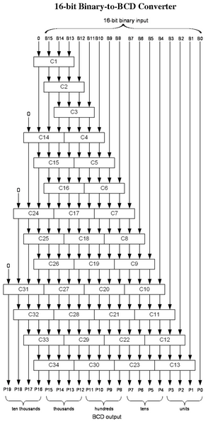
This describes a series of "Add-3 Units", which are combinational logic components with 4 input and output bits. If the input>=5, then the output is the input+3. Else, the output is the same as the input. Naturally, I created one of these units in Logic Land, and then sent it to 'Dan' with these schematics (which he had to flip upside down himself), and told him to recreate the wires. I then discovered that the add-3 unit was defective, so his time was wasted. His result was stupid anyway, so I made a proper add-3 unit and did the whole thing myself.
I don't understand how it works, but it does, so I use it.
The displays themselves use a 4-bit DMUX to take BCD values as addresses to read from a small ROM component 10 rows tall, 7 columns wide. It has the values all 7 segments should be in given any of the 10 possible decimal digits. It was based on this.