323
A 32-bit computer constructed in Conway's Game of Life with a luxurious instruction set. By blah 2022-2024. My 4th computer.

The 323 is a 32-bit load-store architecture CPU with 14-16 GPRs (depending on how you count), and many 3-argument arithmetic and logical instructions that allow you to specify 2 source registers and a destination. Only loads and jumps can use immediate values; all other instructions exclusively use registers. You can play Tetris on it.
HOW TO USE: The 323 can be run in a Game of Life simulator like Golly. First download 323.mc, load-prog.lua, and 323.lua. Open 323.mc in Golly, and then, without advancing the simulation, run load-prog.lua. It will prompt you to select a .323 file containing code to assemble and load into the machine; find example .323 files here.
Once a programme is loaded into the machine, you may want to make sure you're looking at the display before you run it. It's at the left, below the CPU. Set the scale to 2^4:1, so the pixels will display optimally.
Some images are links; they link to .mc files that can be run in Golly. You can copy them from your browser and paste them into Golly with ctrl-shift-O.
Thank you to Rei for providing corrections to this documentation. They also wrote an emulator.
Table of Contents
Why?
Large patterns in cellular automata are typically simulated using the HashLife algorithm, or some variant of it. Most of these patterns are not optimised for HashLife in particular, and to my knowledge no HashLife-optimised computers had ever been built. I believed that a computer built from the ground up with HashLife in mind could run at incredible speeds; I was disappointed when I discovered that my machine only goes at a few hundred hertz when run in a HashLife implementation. Nevertheless, I decided to put in the effort to make a complete CPU with a reasonably complete instruction set, so that I could have fun programming it. For speed, I could use an emulator. (At time of writing, this emulator is still a work-in-progress.)
I learned the hard way that if you put less effort into the CPU, you simply have to put more effort into programming it. There are plenty of hobbyist CPUs out there which are borderline impossible to programme. The creator writes some simple programmes, culminating in a prime number generator (if that), and then gets bored. With the 323, I avoided that fate by actually putting in the effort to make a good CPU.
The 323 builds on lessons I learned from making my other CPUs. Of all the computers I've designed, it is the most fun to programme. It's also the most complicated. As for the more broad question of why I design CPUs in the first place: Why does anyone do anything?
How?
I already knew that the most well-known programme for this sort of thing, Golly, was not up to the task, since its interface is designed to pretend HashLife doesn't exist. It gives the illusion of a flat 2D array of cells, and doesn't allow you to directly edit hash-nodes on a larger scale. Besides, I always felt that Golly makes for a terrible circuit editor. So in late 2022 I started working on my own programme, thl, which is a text-mode programme; that is, it runs in a terminal, without a GUI, and has no mouse support. It's stil a work-in-progress, and I'm not comfortable posting it yet. For now I'm keeping thl to myself.
At this point, I have to explain how HashLife works. The simple way to simulate a cellular automaton is to have a 2D array of cells and just iterate over them, calculating their state in the next step. You then realise that most of the universe is empty, or just doing the same thing over and over again, so you try to make it recognise those repeating patterns and ignore them, only simulating the parts that are actually doing something interesting. HashLife is essentially a generalisation of this idea. Rather than needing repeating patterns pre-programmed into it in any way, it recognises patterns itself.

It does this by using a compressed representation of space and time, in the form of what's called a canonicalised quadtree. I'll start by explaining space. In the diagram on the left, you see a 4x4 region, which can be subdivided into 4 2x2 quadrants, as shown to its right. We can thus represent the 4x4 on the left as an ordered list of 4 pointers, each pointing to a 2x2 region. So far this seems pointlessly complicated, but here's the clever bit: Some of them may be the same - in this case, the first two are both just empty - so that empty 2x2 only needs to be represented once in memory. As such, the two pointers to the top quadrants are the same. This can be repeated on larger scales; an 8x8 is just 4 pointers to 4x4s, and if 2 or more of those 4x4s are the same, they are only represented once in memory. In addition, if a 2x2 occurs in multiple 4x4s, that 2x2 is still only represented once, even if there is no 4x4 in which it occurs more than once (and so on for 4x4s that occur in more than one 8x8, etc.). With this approach, patterns of exponential size can be represented in only a few kilobytes of RAM, rather than terabytes, assuming that they contain sufficient spatial repetition.
The term for one of these square regions is a node (or "hash-node" / "hash-tile"). Each node points to 4 smaller sub-nodes, unless it's a cell. The size is referred to as depth; a 1x1 node, also called a leaf node or a cell, has depth 0. A 2x2 has depth 1, 4x4 is depth 2, etc. So a depth n cell has a side length of 2n, and an area of (2n)2 = (22)n = 4n. It points to either no nodes at all, or to 4 nodes of depth n-1.
So then how do we represent time? Well, first of all, the simple, non-HashLife way to do this is to only store the pattern at one particular point in time. The advancement of time is thus represented trivially by actually changing the in-memory representation itself. HashLife doesn't do that. It stores space and time, basically in 3 dimensions.
I lied, by the way. A node is not a list of only 4 pointers, there's actually a 5th one, called RESULT. It points to a node storing the result of simulating that node for some amount of time. There's a problem, though: In order to know what the future state of a region of space is, you need to know its surroundings. Each node may occur in many places, but is only represented once in memory, and can thus have only one RESULT.
However, we can know what the centre of that node will be at some point in the future. For example, if we have a 4x4, then we can figure out what the 2x2 region in its centre will be after 1 step of simulation. If we have an 8x8, we know the centre 4x4 after 2 steps. In mathematical terms, if a node has depth n, then its RESULT has depth n-1, and represents the centre of the main node after 2n-2 steps.
We can compute RESULTs recursively. The amount of time that the RESULT advances through, for a given node, is two times the corresponding amount for its sub-nodes. We can thus stitch together the RESULT of a node by taking the RESULTs of nodes with a depth one lower in two stages. See the following set of 4 diagrams of a depth n node:

The last one is our goal, with a single depth n-1 RESULT in solid black in the centre, advanced by 2n-2 steps. In the first, each depth n-1 quadrant has a RESULT, which is solid black, and advanced by only 2n-3 steps. We want to create a 3x3 region of such nodes, as in the 3rd diagram, for reasons that will become apparent, and so to do that we need to fill in the remaining plus shape in the middle. We do that using the sort of construction seen in the second diagram.
The shaded area is produced by creating a new node that contains some of the depth n-2 nodes (separated by dotted lines) of our main node, and is not advanced in time. Its RESULT fills in the gap between the top two RESULTs in the 1st diagram. We do the same sort of thing for the remaining 4.
With this 3x3 of depth n-2 nodes, we can advance further. Using a similar sort of construction to the 2nd diagram, we create a node that contains the 4 nodes in the top-left of the 3x3, and then the 4 on the top-right, then bottom-left, and then bottom-right. We generate all 4 of their RESULTs. Each of these RESULTs is now a quadrant of the final RESULT in the last diagram, which is constructed through the same means as the shaded area in the 2nd diagram, using the aforementioned 4 RESULTs.
Not all nodes need to have RESULTs stored. If the RESULT is not already present, it will be calculated using the above algorithm, until we reach a 4x4, in which case we just apply the transition function of the cellular automaton itself (in our case, Conway's Game of Life). But after the RESULT has been calculated once, it does not need to be calculated again. This is the key to HashLife's performance; it means that we don't need to simulate the same thing multiple times.
A few observations about this algorithm:
- It runs at the same speed regardless of the spatial size of the nodes; it doesn't care if it's working with 4x4s or regions of trillions of cells, as long as their RESULTs are known.
- It works better when structures are aligned to powers of 2, spatially and temporally, because then the nodes line up properly so they can be the same. Note that 2n, where n>0, is only divisible by other powers of 2.
- To maximise speed of simulation, you want to reduce the amount of new nodes that get created. If you have a random 32-bit signal travelling around the machine, it will create new nodes wherever it goes. However, if the exact same 32-bit signal, with the same bits, travels around the same place again in the same way, it doesn't necessarily create any new nodes. Throughout this document, I use the term "novel data" to refer to the former case, and "non-novel data" to refer to the latter case. (This part is important; make sure you understand it.)
- Experience has shown that it can be surprisingly difficult to predict the performance of HashLife intuitively. It simply doesn't conform very well to how the human brain perceives space and time.
Anyway, back to thl. The interface allows you to pan the camera and move a cursor around, and copy/paste rectangular selections. Most importantly, it allows you to zoom in and out and operate on nodes at any chosen zoom level, referred to as z. At z=0, each character in the terminal is a cell. At z=1, each character is a 2x2 of cells, etc. The selection tool also accomodates this; if you copy/paste a 5x5 region at zoom 10, it takes the same amount of time to do so as if you did it at z=0, despite the fact that you are copying 410 times as many cells. No other programme to my knowledge has this feature.
thl is best used with a font where the characters are square. I use it in the Linux framebuffer console with the drdos8x8 font, with which it looks like this:

Without describing it in unnecessary detail, thl has one more important feature: Node symbols. As you can see in the image above, nodes in which all cells are dead are displayed as space characters. Others are displayed as random white upper-case characters. The same node will be displayed as the same upper-case character (although it may change between different invocations of the programme). However, some have node symbols, which can be any character and any colour; they are specified in the file itself, and are persistent. This makes it easy to recognise commonly copy/pasted components.
Fundamental components
In 2023, I began working on a set of components that could be copy/pasted to make a computer. Much of the 323 was made out of these components. Does that mean it isn't really made in the Game of Life, but instead an abstracted cellular automaton with nodes in a higher depth? Well, maybe it would if I was never forced to zoom in and work with individual cells, but in practice these components were often more of a starting point than anything else. As you can see in the above screenshot, there are many un-symboled nodes.


First off, I knew I had to use power-of-2 periods, both temporally and spatially. I also made the decision to use LWSSes for my signals, although for much of the circuitry I ended up working with gliders anyway. I wanted LWSSes to be able to pass between each other, without colliding, and the lowest power-of-2 period that allows this is p64. As such, pretty much the entire computer is built with p64 circuitry. First of all, I found the p32 gun pictured at the left. I also found the p64 one pictured on the right. I then needed an LWSS gun. I used 3 p32 glider guns to create a p32 LWSS gun and then added another p32 to kill every other LWSS, making it p64. I also used the p64 guns to create 2 fundamental switching components, from which, in addition to the LWSS gun, all logical operations can be derived. This basic circuitry toolkit is demonstrated here:

I recommend watching the above pattern in operation. There's an LWSS gun on the left, and two on the top. As the rightward-travelling LWSSes pass through the switching components, they cause the output below to change. So both of those 2 components have 2 inputs and 2 outputs. 1 output, the one to the right, is simply the same as its input on the left; the rightward LWSSes pass through unchanged. The ones going down, though, either get killed or pass through safely depending on whether there's a rightward-travelling one.
Let's examine their behaviour, starting with the one on the left. At first, the LWSSes trying to go downwards get killed by gliders, but then another stream of LWSSes comes along and kills the gliders that kill the other LWSSes, allowing them to pass through. This means that the downward stream is the AND of the two inputs. Because it can be used to duplicate a stream into multiple copies of itself, I call it a splitter, denoted in thl's node symbols with the letter s, as you see in that thl screenshot up there.
The other one, however, has an extra glider gun. As such, instead of killing the gliders that kill the LWSSes, the rightward LWSSes kill the gliders that kill the gliders that kill the LWSSes. This extra layer of indirection inverts the function, making it an ANDNOT. This is an inverter, whose node symbols use the letter I.
They say that you can derive all possible logical operations from ANDNOT, so you don't strictly need anything else. That might be true when you're writing logical equations on paper, but I needed to be able to split a signal in two, rotate it 90 degrees, delay it, etc. So that's why we have 2 fundamental components; I don't think just inverters alone would be sufficient.
The components have mirrored and rotated versions, too. The rotated versions have node symbols of different colours, and the mirrored ones use upper-case instead of lower-case. The LWSS guns are indicated with + symbols, and have no mirrored forms. There are also nodes with eaters on all 4 sides, and nothing else; these are to end LWSS streams coming from any direction and have a single full stop as their node symbol. Here's what the above pattern looks like in thl:

Bear in mind, the rotated/mirrored versions of components had to be specifically aligned and adjusted so that they all work properly together; it's more than just simple transformations on the nodes.
These nodes are depth-7, that is, they are 128x128 regions of space aligned with the grid of hash-nodes at that depth. They operate at p64, and use LWSS signals. 4 LWSSes can fit in a single depth-7 node. As you may know, 4 bits is the amount of information encoded by a single hexadecimal digit, and as such, the symbols for nodes containing only LWSSes are hexadecimal digits that indicate the value encoded in the presence or absence of LWSSes, in the same colour as the gun (+) that produced them.
Orange is down. Red is right. Green is up. Blue is left. That goes for guns and LWSSes (as '+'s and hexadecimal digits, respectively). The splitters and inverters are harder to remember, so personally I don't bother; you can just infer them from the context, and watch them in action if you need to.

I also made a simple XOR gate, shown left (clickable, in case you didn't notice). It's just 2 LWSS streams going up to a glider stream; if both LWSSes are present, they mutually annihilate and leave the glider intact. If neither are present, obviously the glider is intact. But if only one is present, it hits the glider and kills it. Note that normally the LWSS guns are timed such that the LWSSes don't collide, so this requires unusual LWSS timing.
I also made a rather interesting component that doesn't require special timing. I call it the carry mechanism, since I originally designed it for use in an adder; its job was to carry ones over to the left. It is, in essence, an S/R (set/reset) latch.

Normally, there are LWSSes coming in from the right and the bottom. The mechanism can be in one of two states: One in which the LWSSes from the right pass through unharmed, and one in which they are killed. The absence of an LWSS from the right causes subsequent ones to be destroyed, thus "resetting" the latch. The absence of an LWSS from below reverses this. To understand how it works, I recommend simply watching it in action.
The are also many cases where I need to take a single LWSS and turn it into 32 or 64 LWSSes in a row. I use the carry mechanism to do this; I just set it and then reset it 32 bits later:

That picture is of the 32-bit one. There's also a 64-bit one; it's just the same thing, but bigger. There's also a demultiplexer (DMUX):

A DMUX is a component that has a number of outputs, and takes as input an address. The address specifies an output, to which a signal is sent. This DMUX works by splitting the address (top input) into its constituent bits, with each bit having its own column. Each row is a possible value that the address is compared to, and if a match is found, a signal is sent. Timing is controlled by an activation signal (bottom input). The left-most column is used to prevent address 0 from being permanently on. The address in the above pattern is 111 (in binary); try removing LWSSes from the address and seeing how it changes the result.
With some (though not all) basic components worked out, I started working on a computer. I called it the 3232323, since it was a 32-bit computer in the Game of Life (often known by its rulestring, B3/S23), and work began in 2023. I often refer to it by the first 3 numerals, for brevity. Rather than describe the entire process in detail, I will instead describe the architecture and then the implementation.
Architecture
"On two occasions I have been asked, - 'Pray, Mr. Babbage, if you put into the machine wrong figures, will the right answers come out?' In one case a member of the Upper, and in the other a member of the Lower, House put this question. I am not able rightly to apprehend the kind of confusion of ideas that could provoke such a question." - Charles Babbage, Passages from the Life of a Philosopher, 1864.
The 323 is RISC, whatever that means. It uses a 32-bit load-store von-Neumann architecture. The machine state at any given point is comprised of 15 32-bit registers, the PC, the flag (1 bit), the cache, and the RAM.
The size of the PC and cache addresses are difficult to measure. The RAM only goes up to address 1FFF, and then loops around; the RAM ignores the high bits of any address sent to it. The PC can very well hold much higher values, though, and there is no way for the programme to know if this has happened. For the sake of simplicity (and allowing emulators to easily add more RAM), I simply call them 32-bit.
RAM addresses 0-127 are invalid, and any attempt to access them results in the machine halting. This is referred to as a memfault. The reason for this is to make it easier to spot bugs, where a null pointer or random small numeric value is accidentally used as an address.
Numbers are represented in two's complement. All jumps use absolute hword-based addresses. A hword (half-word) is 16 bits.
Instructions
The instructions are 16 bits long, not counting immediates. The RAM is word-addressable; it works in units of 32 bits. As such, the PC addresses are shifted by 1, with the rightmost bit indicating which hword of a word the instruction will be read from (the rightmost (least significant) hword of a word has a lower address, and is thus executed first). As such, for the purposes of instruction decoding, the ram is hword-addressable.
4 bits are used in an opcode to specify a register. In assembly, these registers are named with the letter "x" (pronounced "cross") followed by a hexadecimal digit, which, if greater than 9, must be upper-case. x0 (pronounced "cross nought") is a special register; attempts to read from it will always return 0, and attempts to write to it do nothing. Attempts to write to xF will result in the value being inverted (that is, bitwise NOT). All other registers are normal.
Some instructions contain immediate values. In the following table, they are referred to as IMM16 (immediate hword) or IMM32 (immediate word). IMM32s do not need to be word-aligned, they are hword-aligned. The least-significant hword comes first.
Flag values only last for 1 instruction. An instruction that sets the flag must immediately be followed by a conditional jump if the resultant flag value is to be used. If the flag value is not mentioned in the "function" column then the instruction sets the flag to 0. INZ stands for "is not zero", meaning the flag will be 1 if there is at least one non-zero bit in the result of the operation's calculation.
Here are the instructions. The opcode hword can be best understood as a set of 4 nybbles. The letters X, Y, and Z are used to represent the nybbles at certain locations; they should be substituted for the actual contents of that nybble. For example, "add x1,x2,x3" is assembled to 0x0123; "st xC,x0" becomes 0xa0c0, etc.
| assembly | opcode | function | notes |
|---|---|---|---|
| add xX,xY,xZ | 0XYZ | xZ = xX + xY; flag = overflow | |
| sub xY,xX,xZ | 1XYZ | xZ = xY - xX; flag = xY >= xX | Note that the first 2 operands in the assembly are reversed with respect to the opcode hword. This is so that they appear in the same order as in the expression (xY - xX); otherwise it was confusing. |
| mul xX,xY,xZ | 2XYZ | xZ = xX * xY; flag = overflow | |
| div xX,xY,xZ | 3XYZ | xZ = xX / xY; flag = INZ | Unsigned integer division; overflow is impossible. Division by 0 returns -1. |
| mod xX,xY,xZ | 4XYZ | xZ = xX % xY; flag = INZ | Again, unsigned. If xY is 0, returns xX unchanged. |
| shf xX,xY,xZ | 7XYZ | xZ = xX shifted logically by xY | These 3 instructions (shf, sha, and rot) use the rightmost 6 bits of xY as a signed two's-complement integer indicating the amount. A positive number means shift/rotate to the left, and a negative one is to the right. |
| rot xX,xY,xZ | 8XYZ | xZ = xX rotated by xY | See note on shf. |
| sha xX,xY,xZ | 9XYZ | xZ = xX shifted arithmetically by xY | See note on shf. |
| or xX,xY,xZ | bXYZ | xZ = xX | xY; flag = INZ | |
| and xX,xY,xZ | cXYZ | xZ = xX & xY; flag = INZ | |
| xor xX,xY,xZ | dXYZ | xZ = xX ^ xY; flag = INZ | Can be used to check if 2 registers are equal. |
| st xY,xX | aXY0 | Store xY to RAM address xX. | AKA STR. |
| out xX,xY | aXY1 | Write xX to I/O pin xY; flag set by peripheral. | See section on I/O. |
| jmp IMM16 | e000 IMM16 | PC = IMM16 | AKA JMPI. |
| jnf IMM16 | e001 IMM16 | If flag is 0, PC = IMM16 | AKA JNFI. |
| jf IMM16 | e002 IMM16 | If flag is 1, PC = IMM16 | AKA JFI. |
| ld IMM32,xZ | e01Z IMM32 | xZ = IMM32 | AKA LDI. This instruction is rather common, since most of the others can't use immediates. |
| ld xY,xZ | e1YZ | xZ = contents of RAM address xY. | AKA LDR. |
| jmp xY | e2Y0 | PC = xY | AKA JMPR. |
| jnf xY | e2Y1 | If flag is 0, PC = xY | AKA JNFR. |
| jf xY | e2Y2 | If flag is 1, PC = xY | AKA JFR. |
| in xY,xZ | e3YZ | Receive word from I/O pin xY and write to xZ; flag set by peripheral. | See section on I/O. |
| hlt | eeee | Halt the machine. | Opcode chosen because it's like a panicking noise. However, this can just as well be used for successful termination of a programme, in which case I suppose it's a squeal of joy. |
Maybe that doesn't seem luxurious to you, since some things you may be used to in other architectures are missing. If you take the time to learn to programme the 323, though, you'll find all the needed functions follow quite simply from this instruction set.
There is no MOV instruction, since "mov A,B" can simply be done with "xor x0,A,B".
There are no comparison operations, because sub and xor, with a destination of x0, already serve this purpose. In fact, the operations >, <, >=, and <= can be done with only a single sub, by reversing the operands and inverting the conditional that follows (i.e. replacing jf with jnf or vice versa).
There's no ADC or SBB, but why would you need them? I think ADC is only really useful for 8-bit or 16-bit architectures, when the word size is too small. Ask yourself, though: How often do you actually need more than 32 bits in an integer? Sometimes, I suppose, you need 64 bits to index into a large array. The 323 doesn't support a large enough RAM size for that, though. On many modern architectures, in C, an "int" is 32 bits, and that works just fine.
Cache
The 323 has an LRU instruction cache, although there is no data cache. Instructions are never read from RAM directly; they can only be read from the cache. The cache consists of 4 16-word lines, each of which has an associated address and position in the £O (cache order).
The ST and LD instructions access RAM directly, without any cache. There is no attempt made at cache coherency, since the only use of updating the cache would be self-modifying code, which is an obscure use case. A cache line's contents do not change until it is rewritten by a cache miss, with a new corresponding address. Of course, if you really want, you can use the following "clr" function to clear the cache:
        align 32
clr:    jmp clr2
        align 32
clr2:   jmp clr3
        align 32
clr3:   jmp clr4
        align 32
clr4:   jmp xC
        align 32
This function uses the assembler's "align" directive to reserve enough space to fill up all 4 cache lines, which are 32 hwords long and aligned to 32-hword boundaries, and then it uses unconditional jumps to go between them, thus clearing out all previous cache lines, before jumping to a return address in xC. Of course, this function doesn't refresh the entire cache if one of its own cache-line-sized areas is in there, but is guaranteed to clear out any others.
It may be desirable to make a cache line un-hittable, to represent that it has not yet been filled in with anything. The load-prog.lua script does this to initialise the programme, by setting one of the low 5 bits of the cache line address to 1, which is normally impossible, since the address refers to the beginning of a cache line. As such, it can never possibly match any possible cache line address, and so will simply remain un-hit until it is filled in. A cache line address of <256 is invalid and cannot occur.
Assembler
I wrote an assembler in Lua, which is provided as part of load-prog.lua (see "HOW TO USE" above). It is rather simple and doesn't support file inclusion or macros, but it serves my purposes well enough. Each line consists of an optional label followed by an optional instruction or assembler directive. Instructions consist of the opcode mnemonic, whitespace, and then the arguments, separated by commas, with optional whitespace.
The assembler is hword-based. The addresses of labels are PC addresses (hword-based), as are used in JMP instructions. For LD/ST instructions, normally you want word-based ones, which you can do by prepending an '@' to the beginning of the label when using it (but not when defining it). If an '!' is placed before an immediate, then it becomes a "pseudo-immediate", i.e. a LDI instruction is generated to store it in xE. For example, "xor x1,!45,xC" is syntactic sugar for "ld 45,xE" followed by "xor x1,xE,xC". If '@' and '!' are both present, the '!' must come first. Execution starts at the "start" label if present, else the beginning.
The assembler supports the following directives:
- align NUM: Add padding 0s, if needed, to bring us up to the nearest multiple of NUM. If you want to use dw, you probably want to put "align 2" first.
- dh VAL: Declare hword. Inserts the hword VAL into this location.
- dw VAL: Declare word.
- rep VAL AMT: Repeat. Equivalent to repeating "dw VAL" AMT times.
- str STRING: Output a string in my weird format. See text.323. No quotation marks needed.
For nano users, here's a .nanorc file that provides syntax highlighting.
Quick Notes
For debugging purposes, a register's (let's take x1 as an example) contents can be written to the left-most column of the display by doing "out x1,!0xe" and then "out x0,!0xe".
Loops can be implemented by writing the number of desired iterations into a register, subtracting it by 1 at the end, and checking the flag, which will indicate if 0 has been reached or not. The following programme counts down from 31 to 0. The loop body runs 32 times.
start:	ld 31,x1     ; iterator variable
loop:	out x1,!0xe  ; write to display
	out x0,!0xe
	sub x1,!1,x1 ; handle looping
	jf loop
	hlt
The way the 0xe (display) output works is that first, you specify the data to write to a column, and then you specify the column number to write to. If you swap x1 and x0 in the 2 "out" instructions in the above code, it clears the display (fills it with 0s).
The keyboard input pin is 0xd. It returns 0 if no key is being pressed, else the keycode. Right now it just supports the arrow keys (LEFT = -1, UP = -2, RIGHT = -3, DOWN = -4). Here's a programme that displays the currently pressed key:
start:	in !0xd,x1
	out x1,!0xe
	out x0,!0xe
	jmp start
Functions can be written. My personal convention is to store the return address in xC, and to allow functions to clobber (over-write) the high registers (x8-xF), but forbid them from clobbering the low registers (x1-x7). In terms of the CPU/architecture itself, there's nothing special about these registers; it's just a matter of convention, to make code consistent and comprehensible. Calling a function consists of setting xC to the label to jump to after the function's done, and then jumping to the function. For example, here's a programme that calls a function to square a number, and then displays it. Note the comment explaining what the square function does; this documentation takes the place of a function prototype.
start:	ld 5,x1     ; argument to function
	ld ret,xC   ; return address
	jmp square  ; function call
ret:	out x8,!0xe ; write squared number to display
	out x0,!0xe
	hlt

; function that returns x1 squared in x8
square:	mul x1,x1,x8
	jmp xC
These are all just guidelines, and I myself sometimes break them. There are obvious limitations here, as well. What if a function calls another function? They both use the high registers, so they might step on each others' toes. This is to say nothing of recursion. However, I have found in practice that these conventions tend to result in more readable code. I'm sure seasoned assembly veterans would have their own opinions. For examples of recursion, see sort.323.
Once you've gotten the hang of the basics, I recommend looking at text.323. It contains very useful text rendering functions, including one that prints an integer in decimal. This makes it easy to write programmes that do more than just put binary numbers into columns.
Design
 £RD
Instruction
£RD
InstructionDecoder Clock £RA £LD £O RAM
Controller £LSs PC IHC Flag Registers ALU Display I/O RAM
Control Unit (CU)
"Sometimes I think the only universal in the computing field is the fetch-execute cycle." - Alan Perlis, Epigrams in Programming, 1982.
I use the term CU here to refer to the circuitry that initiates an instruction hword fetch, as well as the instruction decoder and the circuitry for handling immediates. Whilst building the machine, though, I never thought of the CU as a discrete component; I don't think I ever even thought to call it the CU. It's just a bunch of control cicuitry that I'm grouping together for the purposes of exposition.
When a clock cycle output is sent, a hword fetch occurs. This may either be a cache hit, in which case it is sent to the cache read dispatcher (£RD), or a cache miss, in which case the clock is stopped until a cache line is filled. The next hword fetch after a cache miss will always be a cache hit, unless a memfault occurred, in which case the clock is never un-paused and the machine halts.
Clock
All operation of the machine starts ultimately with the clock. It is at the very heart of the 323, nestled beneath the cache reading circuitry. On the face of it, the clock seems to have a very simple, even trivial, purpose: Send out a signal every so often, at regular intervals. However, some instructions take longer than others, so they have to be able to tell the clock to wait for longer than usual. Others still, such as memory access or I/O instructions, take an unknown amount of time, so they must stop the clock indefinitely, until a signal comes along to un-stop it.
The clock consists of a bunch of circuitry fed by the following simple mechanism, the "clock of the clock" if you will:


It's just 11 semi-snarks fed by a p64 gun. Each semi-snark doubles the period, thus resulting in a final output glider once every 217 generations. This is the smallest power of 2 that didn't break anything. The resulting clock signal is converted from a glider to an LWSS travelling to the left.
You can see this in the thl image at left; the "IL" on the right is the initial signal generator that we saw in the previous image, and the blue '+' below it generates the resultant LWSS. It then goes through an AND gate, which we see here as a lower-case green 's'. What signal is it being ANDed with, you ask? The answer is a carry-mechanism latch which indicates whether or not the clock is halted, which can be cleared by the microcode to stop the clock, or un-cleared by several other parts of the machine to restart it. If the clock is stopped, the signal ends there and we wait until the next time to have another go.
After that, the signal goes through a series of 4 T-flip-flops, which allow for further delays depending on the previous instruction which was executed. They are automatically reset to all 1s after a clock signal makes it through them, and each bit can be zeroed individually by an instruction's microcode.
If the clock signal makes it through all that unscathed, it leaves the clock and triggers a hword fetch. It also increments the PC if there's a cache hit. If a jump instruction occurs, the PC is written to after having been incremented, thus rendering the incrementation pointless. We will first describe the PC, because it is simpler.
Programme Counter (PC)

The PC has the following functions:
- Read value (with low 5 bits cleared) into cache line selectors, and read unaltered PC to the cache read DMUX (which only uses its first 5 bits).
- Increment.
- Re-write from immediate or register. (To do this, the PC must first be cleared.)
The first function is always being done at all times, because there is no reason not to; nothing bad happens if the PC is read when it doesn't need to be read, and so I simplified the circuitry by not bothering with an explicit "it's time to read the PC" signal. The low 5 bits are cleared (because we're selecting a cache line, not an address within one) by ANDNOTing it with a loop.
The second is triggered by a signal from the £LSs; if a cache hit occurred, the PC is incremented, else it is left alone. This signal is a single LWSS which is fed into a carry mechanism at the top right, producing a stream of 1s of a certain length, which depends on the contents of PC; this stream of 1s is then fed into an XOR gate in the PC, and thus has the effect of adding 1 to the value.
The third function is served by some inputs at the bottom and one at the left. There's a 32-bit signal generator to the bottom left of the PC which clears it, and then there are another 2 inputs to set some of those 0s to 1s, thus writing the new value. One is on the left, and writes a register value. The other is at the bottom, and writes an immediate value.
Cache Line Selectors (£LSs)

A hword fetch starts with taking the high bits of the PC and using it to select a cache line, or to fetch an entire cache line if there was no match. I'll leave a discussion of cache misses for later. For now I will address cache hits.
There are four £LSs, one for each cache line. Each holds an address which is XORed with the high bits of the PC; an activation signal from the clock sets a carry mechanism latch, which is then reset if there's a non-zero output from the XOR. That is to say, the latch will only remain set if the address in the £LS is the same as the high bits of the PC. If the PC is incremented too soon, it may cause the latch to be reset too early if it crosses a cache boundary, so the PC increment signal is delayed; you can watch it go up and then back down if you know where to look (to the left of the £LSs).
If a £LS is selected, it sends a stream of LWSSes to the right, which is used for reading. The CU also checks to see if none of the £LSs matched, in which case it triggers a cache fetch, or alternately allows the PC to be incremented.
Cache Reading Area (£RA)

Once a £LS has been activated, it sends LWSSes off to the right, into the £RA, and these LWSSes select the cache line to be read. The PC is then sent into the DMUX at the bottom of the above image to select a column. Only the low 5 bits are used. We want to read 16 bits, but the DMUX normally just outputs a single LWSS, so we use a series of glider guns and reflectors to make the absence of a single LWSS in one of the address bit rows turn into the absence of 16 LWSSes. It basically ANDs the stream with itself shifted by greater values. For example, ...111101111... Becomes ...111100111... if you AND it with itself shifted right by one, and then if you do that again, shifting by 2, it becomes ...111100001... and so on.
So the DMUX produces 16 LWSSes going up in the column we want to read. There are 4 cache lines, all of which are constantly feeding their data, in the form of LWSSes, into the £RA from the right. The cache line which is selected by a £LS is the one that gets read. The exact data which is read thus depends on timing; if the read signal is sent 16 "ticks" (units of 64 generations, corresponding to 1 bit) later, then a different hword will be read. As it happens, each column is 256 cells wide, which is 8 bits long, since each LWSS is separated by 32 cells. Since the address going through the DMUX goes to the right, whereas the cache data goes to the left, it turns out that this results in the offset of bits read between 2 adjacent columns being exactly 16 bits, which is what we want.
The hword which was read goes up to the top, then over to the right and down the right side of the £RA. Since the distance to the top right is the same regardless of which column was selected, the timing is the same every time. This is by design. Also, an activation signal in the form of a single LWSS goes with it. This activation signal, along with the hword itself, then encounters the £RD.
Cache Read Dispatcher (£RD)

The £RD is responsible for choosing whether to send a hword read from the cache to the instruction decoder or the immediate handling circuitry. It does this with 2 latches and some ANDs. Only 1 latch is strictly necessary, but I originally intended for it to have more than 2 modes, with 1 latch for each mode. In reality, I ended up using the IHC for that.
The £RD can have its state modified by a microcode column or by the IHC. An LWSS hitting the bottom clears both latches, and then there are 2 wires that set them.
Immediate Handling Circuitry (IHC)

The IHC figures out what to do with an immediate hword. It either just jumps to it directly (as in immediate jumps), it stores the first hword of an immediate word (as in immediate loads), or it interpets it as the second hword of a load and writes the full word to a register. There are thus 3 modes of operation, encoded with 4 latches. As you can see by the labelling in the above image, the right-most latch is useless. I probably expected I would use it for something, but it never turned out to be necessary and I didn't care enough to remove it. The left-most latch is un-labelled.
Jumps are straightforward; just take the hword, write it to the PC, and then reset the £RD to send hwords to the instruction decoder. The loads are more complicated. They start with the second-from-left latch, labelled LDI in the above image, which writes the hword into an internal machine register (top left of image, with 4 'f's). It then switches over to the leftmost latch, which takes the next hword, ORs it with the data in the register, clears the register, and sends the result of the OR down to get written to the destination register. To do this, it triggers the AHR.
Instruction Decoder (ID)

One of the first parts of the machine to be built. The bit at the top splits off the 3 rightmost nybbles of an instruction. The rest is a PLA, although I didn't know that's what they were called when I first made it. The part of the PLA to the right of the image is really just a DMUX with a 16-bit address, where most of the 216 possible rows are missing, and most of the ones that aren't have empty spaces where there would normally be splitters or inverters, meaning that that bit is ignored. For example, LDR has 11100001 = 0xe1, and then 8 empty spaces, which corresponds to the opcode hword for LDR being e1YZ as described in the table in the "Architecture" section above.
The left half of the PLA contains a bunch of columns that are optionally triggered by the presence of an inverter. In other words, a simple microcode. I say "simple" because it's only consulted once per instruction; there are no microcode loops, nor even a 6502-style clock input to the PLA.
The timing of signals on the orange columns is always the exact same, regardless of the row that triggered them. If this were not the case, the machine would've been much harder to build. The green columns do not have this trait, but they don't need it. There's a bunch of empty space to the left because, not knowing how many columns I'd end up needing, I reserved more space for myself than I needed.
I'll number them from 0-18, where the right-most one is 0 and the left-most is 18. The right-most 4 columns specify a 4-bit ALU opcode. Other than those, from right to left, they are:
- Read X.
- Read Y.
- Jump.
- Jump if flag.
- Jump if not flag.
- Special 1.
- Special 2.
- Write destination register address to AHR.
- Delay by 1 cycle.
- Delay by 2 cycles.
- Delay by 4 cycles.
- Delay by 8 cycles.
- Stop clock.
- LDI.
- Jump register.
In thl, re-programming the microcode is incredibly easy; just copy/paste splitters and inverters on the right, and do the same for the inverters on the left. This made some aspects of the design of the CPU much simpler, although I was disappointed by how single-purpose some of the PLA columns are, like the LDI and jump ones.
Columns 9 and 10 specify alternate functionality for pre-existing instructions, based on the ALU opcode. To use conventional terminology, I suppose you could call it a pair of "status" inputs to the ALU. For example, column 10 converts addition to subtraction by inverting one of the operands and adding one.
The 2 nybbles in the middle of an instruction, X and Y, are always fed into the register bank read DMUX with the same timing, but the registers are only actually read if the microcode says so. The destination register, Z, is always sent to the register write DMUX multiple times, but again is only used if an ALU opcode has been triggered. You may wonder why Z is sent more than once; the reason is to simplify the circuitry. Nothing bad happens if you send it when you don't need to (it's non-novel data, so I doubt it even slows down the simulation), so we simply choose when to send a 1-bit write signal, telling the register bank to write a value into xZ. Of course, some instructions take much longer, perhaps an uncertain amount of time, so we want to be able to store Z indefinitely until we need it. That's what the AHR is for.
Register Bank

Basically the first part of the machine that was ever made. It stores the 15 writable registers x1-xF, and allows them to be read and written. Not visible in the above image is the part of the read/write DMUXes in the upper right and lower left, respectively, that break up a 4-bit register address into its constituent bits.
Each register is handled with the following sub-components:

- Read DMUX row, which sends a single LWSS to the left if the address matches. The address bits go down.
- Signal extender, which converts 1 LWSS to 32 LWSSes.
- Memory loop; stores the 32 bits of the register itself.
- Glider gun used for reading.
- Glider gun used for clearing.
- Write DMUX row, same design as for reading, but upside-down. The address bits go up.
- Another 1-to-32 signal extender.
- LWSS gun that duplicates the 32-bit signal from (7), except with considerable delay.
- Inverter. Inputs are (8) and the output of the ALU. Output is to the right.
- Delay for output of (9). Note that only the odd registers have this, but not the even ones.
- Register read bus.
To read, an activation signal is sent to the read DMUX. The register address comes directly from the instruction decoder. It goes through (2) and then (4), which causes LWSSes from (3) to be allowed to go to the left, without being destroyed. They then hit an inverter which is directly connected to (11), thus sending the output down into the ALU. Note that, if 2 read DMUX activation signals are sent 32 bits apart from eachother, the outputs will not collide, since the signals in (11) and (1) are both going in the same direction (down).
To write, an activation signal is sent to the write DMUX. The register address comes either directly from the instruction decoder or from the AHR. It goes through (7) and from there it goes to both (8) and (5). (5) causes the previous contents of the register to be removed. (8) waits long enough to give some time for that to happen, and then goes through (9), thus taking on the value of the ALU output, which is then written to the register directly by colliding with gliders.
Since the signals in (6) go up, rather than down like the other ones, the delay for even/odd registers is different. As such, 16 bits of delay are provided by (10).
The ALU data output goes directly through (9). The stream of LWSSes to its left is the ALU status output, which sets the flag. At one point earlier on, (9) had only one glider gun - making it a splitter - instead of 2, which makes an inverter. This resulted in values being written to registers in inverted form. When I fixed this bug, I decided to leave xF (at the top of the register bank) as it was, to allow for simple NOT functionality with minimal effort.
ALU

The ALU is big and complicated. It does more than what ALUs are normally expected to do; in addition to arithmetic and logical operations, it is involved in I/O and stores/loads. In fact, absolutely all GPR access involves the ALU, since the register bank is connected directly to it.
All use of the ALU involves reading and/or writing one or 2 registers. 1 or 2 values are read, going downwards through the register read bus (RRB), until they reach a bit of value-extracting circuitry which has been activated by a signal sent from the right, triggered by the ALU opcode. Below the right half of the register bank, you can see this extracting circuitry, copy/pasted for each instruction.
The value of a register is assumed to be novel data, so the extractors don't just read it; they also clear the value going down the RRB, so it's just an empty space where 32 LWSSes would be. This means that novel data does not go further down in the ALU than it needs to, thus reducing the amount of hash nodes that are created.
Some ALU operations (like ADD, OR, etc.) are implemented "in-line"; the circuitry to compute them fits in between the RRB and ALU output bus. These operations are fast enough that the AHR is not needed; we simply activate the register write DMUX and write the values immediately. LDI and LDR obviously don't have this property, and neither do DIV, MOD, or MUL, which have their circuitry over to the left. Additionally, the circuitry for SHF, SHA, and ROT is on the right. All of these use the AHR, not because the time they take cannot be predicted (in fact, it's the same every time for any given opcode), but because they all take too long for the normal approach to make sense. You could theoretically just have the destination register address (Z) go through some huge path before ending up at the register read DMUX, but it would be cumbersome.
Now, let's look at those ALU operations one by one, starting at the top.
ADD

The adder consists of a half-adder in the bottom right splitting the input into two streams, the half-sum (A XOR B) and half-carry (A AND B), a carry mechanism, and then an XOR which XORs the half-sum with the carry. You can think of it as a state machine; in the normal state, simply output the half-sum. But if a carry bit is encountered, we keep flipping output bits until we reach a half-sum bit which is 0. That final flipping is done with a small XOR gate.
It may seem strange that the XOR gate in the bottom right is so much bigger than the one at the left; if I already know how to make a smaller one, why would I use a bigger one? The answer is that, as mentioned before, it's a half-adder, which produces both XOR and AND. I don't know of any smaller way to get both of those.
I figured that doing fast addition was of high importance if I wanted the machine to run fast in a simulator, so I went through several iterations of re-designs, did HashLife benchmarks, and optimised this design to death. It's much smaller than my first adder, and takes less time to simulate.
Then I had to attach the adder to the ALU. Since I believed addition to be the most common operation, I decided to put it right below the register bank, so the read-add-write loop would consume as little space (and as few hash-nodes) as possible. I also had to squeeze in some more inputs to allow for subtraction. There's also an input from the microcode that sends a glider with the right timing to set the flag if overflow occurs (you can see this glider go in a zig-zag pattern above the adder). All things considered, the circuitry around this area is some of the most delicate and complicated in the entire machine. I felt like I was carefully walking on eggshells at times, trying not to break anything.
XOR

The adder is complicated and optimised, but this is relatively simple, so I will use it as an example to explain the basic design of an ALU operation.
First, the ALU opcode is decoded and LWSSes are sent to the left from the instruction decoder PLA columns. In this case, two are sent: One is an activation signal for the register write DMUX, and the other goes through some delay, then a 1-to-32 signal extender, and then is used to extract the arguments before clearing them, in the fashion described above.
After the 2 operands are XORed, the output then goes into the ALU data and status output busses (left of above image). The data goes up and then gets written to the destination register. The status ouput is used to set the flag, and it doesn't matter what exactly is sent on the status output; it just matters whether or not there's a gap in the LWSS stream. As such, sending the result of a computation on both the status and data outputs gives you an easy way to set the flag if the result is non-zero. In the case of XOR, this is used to test whether or not 2 values are equal.
There are 3 inverters on the left of the image, 1 for the status output and 2 for the data output. The bottom-right of the 3 has nothing to do with XOR, but is instead used for SHA/SHF/ROT. It would be nice, I suppose, if those instructions set the flag if they produced a non-zero result, and in fact it'd be trivial to make this change. At some point, though, I had to declare the computer done, so that I could write documentation without re-taking a bunch of screenshots and modifying some of the prose every time I make any change. I'd also have to update the emulator. The perfect is the enemy of the good.
SHF/SHA/ROT

All 3 shifting/rotating operations are implemented using the same circuitry. This is done by pre-processing the data to be shifted (which I will simply refer to as the "data", where the other operand is the "shift amount") in a way which depends on the type of operation desired. For SHF, the pre-processed data is just the same as the register value. For ROT, it is repeated 3 times, and for SHA, it is sign-extended to 64 bits. Shifting left or right therefore produces the desired results.
The data goes to the left and then back down, optionally being copied twice by 2 splitters fed by the "special 1" PLA column, or having its last bit extended to 32 bits by a carry mechanism. The data (bottom of above image) and shift amount (above it) then travel to the right, outside of the area normally assigned to the ALU. I did this so that I'd have space on the left for other operations, like DIV/MOD and MUL, basically making a trade-off between horizontal space and vertical space. Here's the bit that does the actual shifting operation:

The data and shift amount enter from the middle left of the image. The data goes through that staircase-looking bit, and the shift amount has its individual bits extracted by a series of splitters and an inverter. The use of an inverter is because it's two's complement, so the value of the most significant bit is inverted. Each of these shift amount bits then goes into a highly compact type of signal extender that uses a clock, and is then used to choose between two different paths to send the data through. One is shorter, the other is longer. First, the difference in delay between the two paths is 1, then 2, then 4, then 8, etc. This thus adds up to the desired shift amount.
After the shifting operation is done, the result is ANDed with a 32-bit signal and sent to the ALU output. I suppose you don't actually need to AND it, but it prevents some novel data from reaching the ALU and register bank.
In the left of the above image, you can see the piece of circuitry that uses the AHR to write data. It's used by every instruction that uses the AHR, not just SHF/SHA/ROT.
AND, OR
See XOR. It's the same thing, with different logical operations.
DIV/MOD

This was a learning experience for me (well, the entire 323 was, but this in particular). I had no idea how to divide 2 numbers in any base, other than using the brute-force "subtract until you hit <=0" approach. If I was taught long division in school, I forgot it. As with everything else, division is easier in binary than in decimal, but explanations of binary division usually assume that you're already familiar with long division in decimal, so here's an explanation that doesn't assume that knowledge, assuming you're already familiar with binary subtraction.
Suppose C = A/B, and that this was calculated in the naive way. Every bit of C represents a power-of-2 amount of times that B was subtracted from A. We can use that fact to optimise things. To determine if a bit in C should be 1 or 0, subtract by B shifted left by the corresponding amount. If the result is negative, the bit is a 0. Else, the bit is one, and we write the new value into A and move on to the next bit.
It's simple to see that this must progress from left-to-right. Stated in pseudocode:
C = 0
FOR I = 31, 0 BEGIN
	B' = B SHIFTED LEFT BY I
	IF A >= B' THEN
		A = A - B'
		C = C OR (1 SHIFTED LEFT BY I)
	DONE
DONE
I used to wonder why the x86 architecture did division and modulus in the same instruction; surely, I thought, it would be more efficient to only generate the one value you need. When we consider this algorithm, we see that the remainder and quotient are both produced at once, so I suppose you may as well give both of them to the programmer. However, I chose to have two separate instructions, requiring the same computation to be performed twice if you want both. Is this less efficient? Well, the data becomes non-novel when you do it twice; the second time, it's just going over hash-nodes that were already computed. The only difference is a latch that chooses which of the two outputs is desired.
It obviously doesn't shift numbers, in the way that the SHF/SHA/ROT circuitry does, every iteration. That would be impractical. It starts with B already shifted to the left and then shifts B right by 1 bit every iteration. Also, we shift C in the same way, instead of shifting the 1 that gets ORed into it.
The DIV/MOD unit has 3 registers, corresponding to the 3 variables in the above pseudocode. C is on the left, A is on top, and B is on the bottom. Since C and B are shifted every iteration, they go in loops that use the same sort of two-way switch which is used for SHF/SHA/ROT, except there's only one of them. It makes the loop 1 bit longer when it's time to shift it. Once the computation is done, all 3 registers are cleared.
MUL

The DIV/MOD unit is probably the one part of the entire machine that I am most proud of. It is in fact my second attempt at making that component, since the first was larger and unwieldy. With MUL, though, I was too lazy to do that, so I just went with the first thing that worked. As such, the circuitry is less optimised. Multiplication is simpler than division, so the algorithm to compute C = A*B is basically:
C = 0
FOR I = 31, 0 BEGIN
	IF BIT I OF B IS 1 THEN
		C = C + (A SHIFTED LEFT BY I)
	DONE
DONE
Again, 3 registers. C is on the left, A is in the middle, and B is on the right. B is shifted, but A and C are not. Every iteration, C is set to the result of itself plus A (if the corresponding bit in B is a 1), or plus 0 (otherwise), shifted left by one bit. It also detects overflow. Since C is shifted to the left, if its left-most bit was a 1, this causes overflow. Furthermore, it might overflow further if a 1 gets carried; as such, 2 bits are ANDed to check for overflow. If either is 1, there is an overflow, and the flag is set. You can see this happen at the left of the circuit if you watch it in action; 2 LWSSes go up though an inverter.
IN/OUT
See section on I/O.
Flag

The flag is a simple S/R latch that stores a 1 or 0. It is cleared at the beginning of every instruction (including jumps, which use the value before it is cleared), and optionally set by some instructions. The signal that sets it is one of the outputs of the ALU, which is used only for this purpose. The flag was designed before I had figured out that you could use the carry mechanism as an S/R latch, so it is needlessly complicated; it has a loop with 32-bit extenders on the inputs. The design is basically an S/R NOR latch.
Cache Line Data (£LD)

This is where the cache lines themselves are located. Each cache line has to store 32 hwords, which is 1024 bits. To save horizontal space, each cache line snakes around a bit. The £LD has to be able to do a few things:
- Read out data to the £RA.
- Allow a cache line to be cleared and then written to.
- Automatically choose which cache line to clear/write.
(1) is always being done, and is trivial. For (2), clearing is done using an input from the bottom left, which is fed using a carry mechanism which is set when a cache fetch starts and cleared shortly before the cache data arrives. For writing, said cache data goes into another input 128 cells to its right, which goes up to the top and then back down to feed into the desired line.
This brings us to (3). How does it know which line to clear/write? This is determined by the £O, which feeds 4 inputs to the £LD from the top, one for each line. The least-recently-used (LRU) has LWSSes going to its corresponding input, and the others have nothing. Signals to clear or write go through splitters that AND them with the corresponding input from the £O.
Cache Order (£O)

The £O is the part of the machine that keeps track of which cache line is the least-recently-used (LRU) one. Each cache line is assigned a unique 2-bit code. The £O is an array of these codes, in which all 4 codes are repesented once, and no two codes are same. It thus has 4! = 24 possible states. When a cache miss occurs, the £O is not actually modified; that only happens when a cache hit occurs, which of course happens in the clock cycle immediately following a cache miss (and associated cache line fetch).
When a cache miss occurs, the data is fetched from RAM, written to the LRU £LD item, and the high bits of the PC are written to the LRU £LS.
When a cache hit occurs, a hword is read by the £RA and the state of the cache is un-modified except for, possibly, the £O. The code for the cache line that was hit is moved to the right. For example, if the £O state is 0321, and cache line 3 is hit, the £O becomes 0213. This is done with a sort of partial shift register. The 2-bit code specifying the cache line that was hit comes from the right of the £O, and passes through, checking for equality with each 2-bit code stored. When equality is found, it sends a signal down, which stops an LWSS stream going to the left, and that stream, finally, indicates which columns should take on the value of the one to their right.
Then the value shifts left up to the point of equality. The hit cache line code is then written to the right-most column. But how does it know the code of the hit cache line? Well, if you look at the bit on the right where those bits come from, they ultimately come from the £LSs. So they give us 4 values, only one of which can be active at a time, and then we have to convert that into a 2-bit value. This is done with a simple bit of wiring to the bottom right of the £O:

The code for the LRU cache line is then demultiplexed into 4 outputs, which go into the £LD and £LSs to tell them which line to modify.
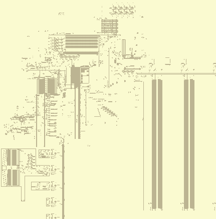
RAM
The RAM is big. Bigger than the entire rest of the machine combined, in fact, as seems to so often be the case when the CPU and RAM are constructed in the same medium. In fact, if you've ever seen a die shot of a recent CPU, a significant chunk of it is taken up by the CPU caches (a sort of lower RAM, if you will). It's surprising just how little of a computer actually computes. Anyway, the RAM in the 323 is divided into 64 columns of 128 words.
Columns
The data storage itself is bascially just the design for the register bank copied and pasted on a larger scale, with the primary difference that, instead of being read/written to using DMUXes, it uses the timing of signals that collide with each other, similar to the WireWorld Computer's RAM (or register bank, as they confusingly call it), if you're familiar with that. It uses this reaction, which I reccomend watching in action:

In the 323, the timing of the signal going up is always the same (for a given column), but the timing of the one on top varies. This therefore causes the point of collision to change, thus selecting a particular row. There are two such timing-based-selector mechanisms in each column. One on the left, which is used for writing and sends LWSSes to the right, and another on the right, which is used for reading and sends signals to the left.
In the register bank, data to be read goes through a downward stream of LWSSes directly to the left of the register data itself. This means that novel data (the register contents) pass right next to the register values, creating a bunch of hash-nodes. That's not much of a problem since the register bank is small, but RAM columns are bigger, so I moved the read output further to the left, nestled in the writing circuitry. It also goes up instead of down. For similar reasons, I moved the first few columns further away from each other, in the hopes that this would reduce the need to create so many hash-nodes, although I've never actually done any measurements to see if this works or not.
RAM Controller

The RAM controller's job is to take an address, an activation signal, possibly a 32-bit data word, and perform the required memory access, depending on whether it is in write mode, normal read mode, or cache line read mode.
The mode of the controller is determined by some carry-mechanism latches. The activation signal and address enter the controller going downwards, from the top left of the above image. The low 7 bits are used to specify the word within a particular column, and the 6 bits to the left of that specify the column itself. Those 6 bits are extracted and travel past the middle-right side of the above image and go through what is basically a normal DMUX, along with an activation signal. This sets some latches that causes the desired column to be selected, and de-selects all others.
The RAM controller contains the following components:
- Address input and activation signal.
- Splitter for high bits (bits 7-12) of address.
- DMUX that calculates fine delay based on least significant 4 bits (bits 0-3) of address, which is put into a loop with specific timing. An activation signal goes up and then back down at a location specified by those 4 bits, and as such they determine the delay.
- 3-bit timer for bits 4-6, adding delay on a larger timescale. This timer counts down and then the loop written to by (3) is read to get a final READ/WRITE signal with more precise timing. It uses the same design as the clock.
- Delay/repeat circuitry, to duplicate a read signal into many copies of itself. Used for cache fetches.
- 32-bit loop that stores data to be written.
- Loop to feed the 3-bit timer. Note that it has the same size as the loop mentioned in (3). This is not a coincidence; it works on higher powers of 2, larger than the time granularity given by (3).
Also note that the amount of time needed for a read/write is determined by the column (bits 7-12 of address), and nothing else. As such, an activation signal is received from the RAM after an access, which arrives with the same timing as any data read, and is sent through this set of latches to choose where to send it based on what the computer wants to do with it:


Memfault indicator
The memfault indicator doesn't strictly serve any functional purpose. It was added when I was working on a fuzzer script for the machine, and I wanted to be able to detect when a halt had occured, and if so, whether it was a memfault or an execution of the HLT instruction (to which end I added a block in the instruction decoder that gets destroyed when a HLT is executed). It's also useful as a visual indicator for humans, though.
It's between the selectors for the two left-most columns, and is triggered when an attempt to access RAM column 0 (which doesn't exist) occurs. On the left you see its normal state, and on the right you see its state when a memfault has occurred, halting the machine.
Input/Output (I/O)
The machine has 16 I/O pins, which are accessed using the IN and OUT instructions. They read register values and use one as an address for a DMUX to select the I/O pin, similarly to that used to select RAM columns, and the OUT instruction also sends register data to write to the selected pin.
Register data is fed to the I/O area here, at the bottom of the ALU:

This circuitry bundles together the relevant inputs (which travel down), with delay for a pin to become selected, and also directs the outputs of the I/O sub-system (Which travel up to the right of its inputs, they appear as green 'f's in the above image) back to the CPU. To understand those inputs and outputs, see this helpfully labelled image:

You can compare the position of the orange 'S'es to the labels to follow the wiring backwards. So from left to right, the inputs to the I/O sub-system are:
- The 4 bits that select the desired pin (actually 5 bits, where the left-most one is an activation signal, which is used to make it so pin 0 isn't always selected).
- 32-bit data input to pin for OUT instructions.
- Activation signal for IN instructions.
- Activation signal for OUT instructions.
And, again from left to right, the outputs:
- Restart clock (this is the only thing that needs to be done when an OUT instruction terminates).
- IN instruction done (we have to write a register).
- 32-bit data to write to register (when executing an IN instruction).
- Set flag.
Those values go to, and come from, the selected peripheral. So as you can see, each peripheral has 3 inputs and 4 outputs. For an IN instruction, IN: ACTIVATE is sent, with no other input. The peripheral must then send IN: DONE and optionally IN: DATA (if IN: DATA is not sent, 0 will be written to the destination register). For an OUT instruction, OUT: ACTIVATE and OUT: DATA are sent. The peripheral must then send OUT: DONE. For both IN and OUT instructions, the flag may be set once an activation signal has been received, using the FLAG output. I put a bunch of non-functional eaters around the peripherals to make it clear where they begin and end.
I will now describe the location and timing of these signals in exact detail, so that others can make their own peripherals for the 323 if they so choose, even without thl. If even one person creates their own peripheral for the 323, I will be deeply flattered.

I will specify exactly when and where LWSSes will appear, all of which will be in one of the phases shown at left. For the leftward-travelling LWSS, the location is defined as the coordinate of the bottom-left-most cell. For the rightward LWSS, it's the bottom-right-most. All times are modulo 213 = 8192, which we represent with t = n * 8192 + x, where x varies between some of the inputs and outputs of a peripheral, and n is some unspecified integer. Also, the I/O pins are spaced at 4096 cell intervals, so the y coordinate of each LWSS varies by p * 4096, where p is the number of the pin (15 for pin F, 2 or pin 2, etc.). All coordinates are as in Golly. Inputs to peripherals are leftward LWSSes and outputs are rightwards.
For an IN instruction, first, at t = n * 8192 + 5760, an LWSS appears at x = -236669, y = -148927 - p * 4096. This is the IN: ACTIVATE signal. The peripheral must then respond to this, do whatever it needs to do, and then produce two outputs.
At t = n * 8192 + 2752, the peripheral must leave an LWSS at x = -236803, y = -150078 - p * 4096. This is the IN: DONE signal. 128 cells below it is the least significant bit of the 32-bit data output, IN: DATA. The more significant bits appear to its left in 32-cell increments. The presence of an LWSS is a 1, and the absence is a 0.
For an OUT instruction, at t = n * 8192 + 2944, an LWSS appears at -235389, -149055 - p * 4096. This is the OUT: ACTIVATE signal. At the same time, the least significant bit of the 32-bit data word sent to the peripheral, OUT: DATA, is at x = -236669, y = -87743 - p * 4096. The more significant bits are to the right, in 32 bit intervals. The presence of an LWSS is a 1, and its absence is a 0.
At t = n * 8192 + 1728, the peripheral must leave an LWSS at x = -236803, y = -150206 - p * 4096. This is OUT: DONE.
All peripherals must produce DONE signals in response to ACTIVATE inputs, otherwise the machine will halt forever, since all I/O is blocking. The 13 I/O pins at the bottom of the machine, as found in the .mc file provided with this documentation, have a kind of "null peripheral" that simply un-blocks the machine but does nothing else.
The other 3 consist of a simple test peripheral that I don't care to document, a keyboard input (see 323.lua), and the display.
Display

The 323 has a 32x32 1-bit colour display, which can be written to by the CPU one column at a time. It cannot be read. The least significant bit of a word goes at the top. Columns are numbered left-to-right, with the left-most being 0 and the right-most being 31. It works by sending LWSSes through a square region, which align to a square grid perfectly every 2048 generations. Note that they are not aligned properly at t=0, but become aligned at t = n * 2048 + 1664, for any n.
Most HashLife implementations colour a pixel/character in as "filled" if it contains at least one cell that isn't dead, and otherwise "empty". Each pixel/character also usually corresponds to a node at a given depth, which is determined by the zoom level. As such, if a small object, like an LWSS, intersects the corner between 4 nodes, it can produce a 2x2 of filled in pixels on the screen at an arbitrarily high depth. This is how the 323's display works.
The design is just, again, the register bank copied and pasted, except simpler since there's no special reading circuitry; all columns are read directly to the display at all times. Note that the even-numbered columns go downwards, but the odd-numbered ones go up. This means the bits of each even-numbered column must be reversed, which is done with this circuitry:
. I guess the reverser itself is reversed.")
It basically implements this algorithm, in pseudocode:
A = WORD TO FLIP
A = (A >> 16) | (A << 16)
A = ((A & 0xff00ff00) >> 8) | ((A & 0x00ff00ff) << 8)
A = ((A & 0xf0f0f0f0) >> 4) | ((A & 0x0f0f0f0f) << 4)
A = ((A & 0xcccccccc) >> 2) | ((A & 0x33333333) << 2)
A = ((A & 0xaaaaaaaa) >> 1) | ((A & 0x55555555) << 1)
In other words, swap the two halves, then swap the quarters within a half, and so on.
Two OUT instructions are needed to write a column of the display. The first gives the data to be written, and the second specifies which column should be written to. As such, there is a register that stores that initial 32-bit value, which is then read and cleared when a second OUT is performed. The display is on pin E (14).